
-
Free consultation hotline
13925432838
13380289778
Address:
Building 1, Qingtang Avenue, Xinnong community, Danzao Town, Foshan City, Guangdong Province, China
Zip:528226
Company Name:Foshan Nanhai Houbo Electronic Technology Co., Ltd.
Operational Address:Liu Yingxiang Workshop II, Xinnongqingtang Development Zone, Danzao Town, Foshan, Guangdong, China
What is Direct Bonded Copper (DBC)
Direct bonded copper (DBC) is a manufacturing process in which copper is bonded to a ceramic substrate, usually aluminum oxide (Al2O3), using a high temperature process. This technology is used to produce a variety of electronic components such as power modules, LED devices and hybrid circuits. It involves bonding copper to a ceramic substrate using a high-temperature process to create a strong and durable bond.
In DBC technology, a thin layer of copper, usually aluminum oxide, is applied to a ceramic substrate through a process called sputtering. The copper layer is then patterned using photolithography to create the desired circuit pattern. The ceramic substrate with the copper layer is then bonded to another piece of copper by a high-temperature process such as diffusion bonding. This creates a strong and reliable bond between the copper and the ceramic substrate.
The DBC process begins with the preparation of the ceramic substrate. The ceramic substrate is first cleaned and then coated with a thin layer of copper by a process called sputtering. Sputtering is a method by which atoms of the source material are ejected and deposited onto the target substrate, forming a thin film. The copper layer is then patterned using photolithography, in which light is used to transfer the circuit pattern to the copper layer.
Once the copper layer is patterned, the ceramic substrate is bonded to another copper piece through a high-temperature process such as diffusion bonding. Diffusion bonding is a solid-state bonding process that brings two metal surfaces into contact at high pressure and temperature, allowing atoms at the interface to diffuse across the boundary and form a strong bond.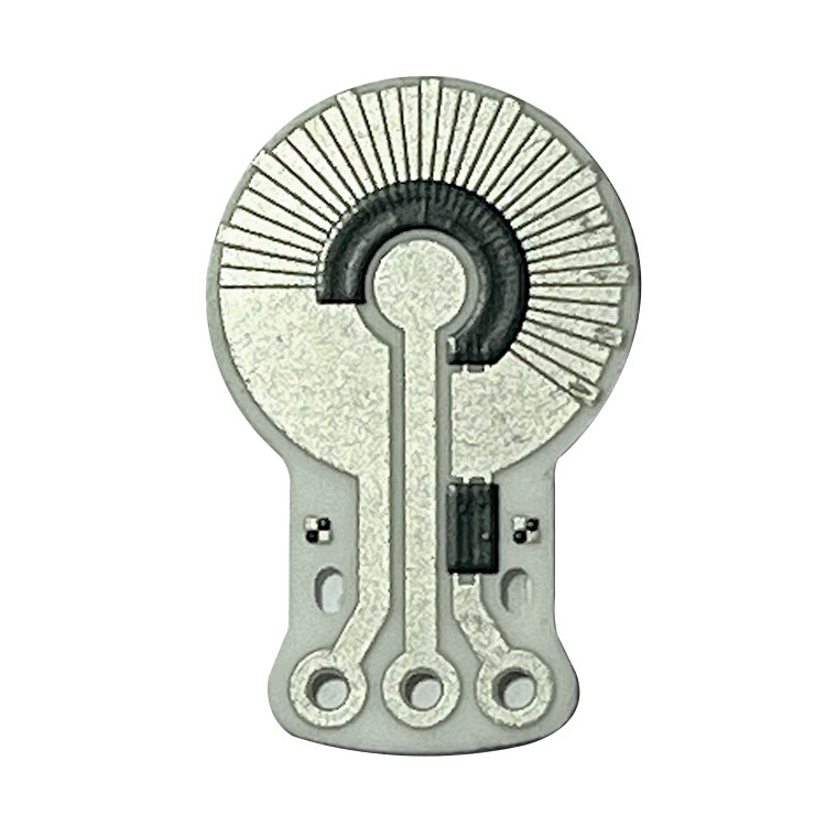 DBC technology has several advantages over traditional printed circuit board (PCB) manufacturing techniques.
High thermal conductivity: Copper has high thermal conductivity, which makes it the best choice for removing heat from electronic devices. Direct bonding ensures that heat is efficiently transferred from the device to the copper layer and then to the substrate.
High reliability: The direct bonding process creates a strong bond between the copper layer and the substrate, which increases the overall reliability of the package. This means that the device is less likely to fail over time due to thermal cycling or mechanical stress.
Low cost: Copper is relatively inexpensive compared to other materials used in electronics packaging, such as gold or silver. In addition, the direct bonding process can be automated, which reduces labor costs and improves process control.
Design flexibility: DBCs allow a wide range of design options, including different substrate materials, copper thicknesses and bonding patterns. This flexibility allows designers to optimize the performance and efficiency of their electronic devices.
Improved electrical performance: The direct bonding process ensures a low resistance path between the device and the substrate, which can improve the electrical performance of the device. This can lead to lower power consumption, faster switching speeds, and improved signal integrity.
In summary, DBC technology has become an important manufacturing technology for many high-power electronic devices due to its superior thermal performance, high design flexibility, and improved reliability. The process involves bonding copper to a ceramic substrate using a high-temperature process and allows complex circuit patterns to be created with high precision and accuracy.

pcb series:Ceramic circuit board | Fuel sender PCB | Printed Resistors PCB | Throttle Position Sensor PCB
Copyright © 2018 Foshan Nanhai Houbo Electronic Technology Co., Ltd.


Address:
Building 1, Qingtang Avenue, Xinnong community, Danzao Town, Foshan City, Guangdong Province, China
Zip:528226
Company Name:Foshan Nanhai Houbo Electronic Technology Co., Ltd.
Operational Address:Liu Yingxiang Workshop II, Xinnongqingtang Development Zone, Danzao Town, Foshan, Guangdong, China
 中文站
中文站
 English